 The gold-plating process
C-Hawk Technology, a global leader in complex manufacturing solutions, delivers industry-leading gold plating through its Arizona-based subsidiary, Gold Tech Industries. The company has supported the semiconductor industry since 1984. It specializes in precision gold plating for multicomponent assemblies used to produce silicon wafers, the base material for nearly all semiconductor devices. GTI’s proprietary gold plating process has set new standards for quality, consistency and performance in epitaxial manufacturing.


Epitaxial manufacturing takes place when silicon wafers are prepared for chipmaking. Gold plating is a key feature of metal components used in specific semiconductor capital equipment, allowing for uniform heating and reflectivity throughout a semiconductor chamber. It also protects the equipment, enhancing the performance and durability of components. GTI’s products have a direct effect on the silicon wafer and are critical to its overall yield and performance, plating aluminum, brass and copper substrates for the epitaxy market.
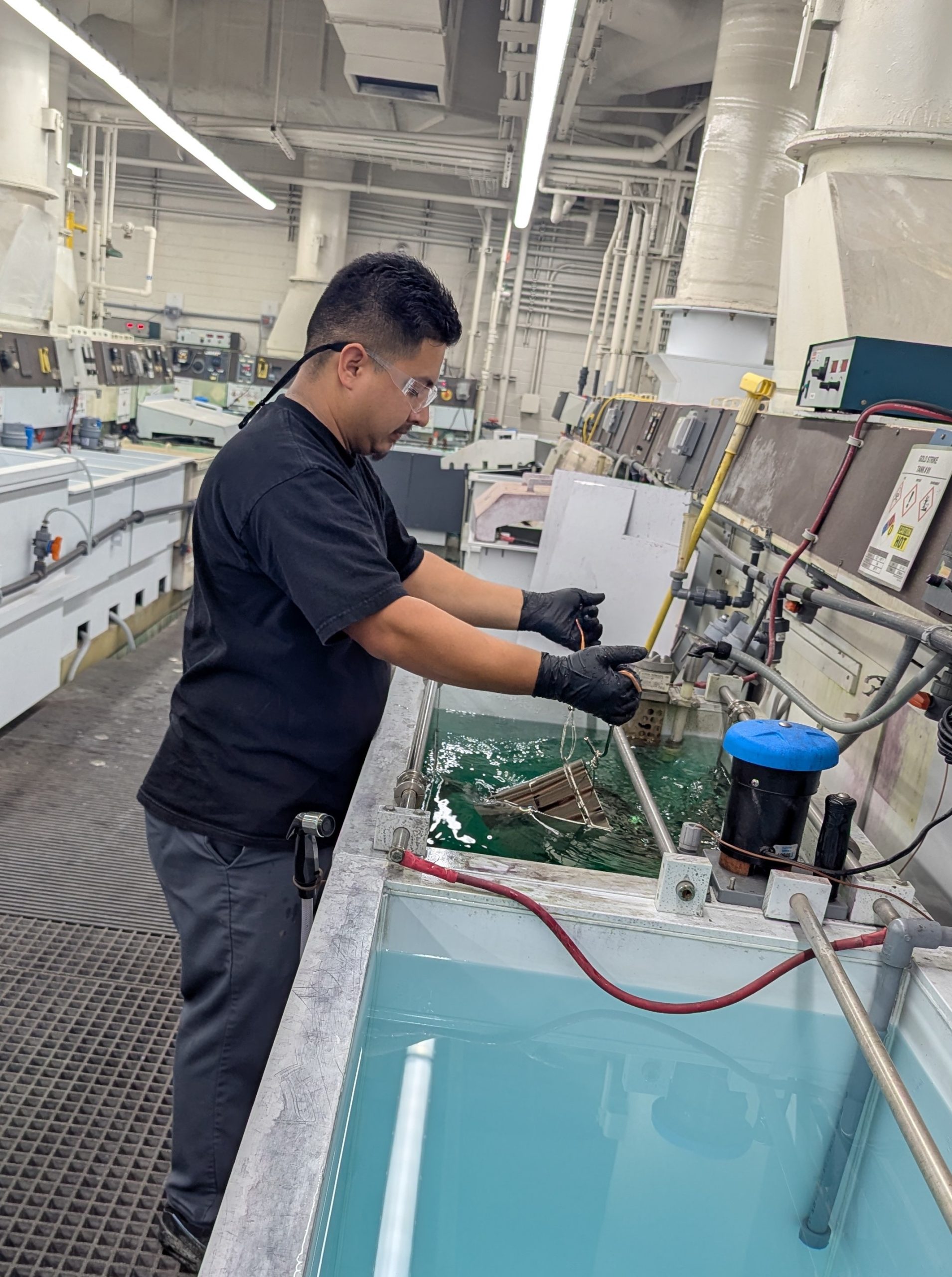
So how does electroplating work? In semiconductor production, reliability often depends on the most minor details. One example is gold plating. The process begins with precision manufacturing and polishing of components to achieve a mirror-like surface. After cleaning, a nickel layer is applied, followed by a uniform gold layer through electroplating. Each component then undergoes strict quality control, including X-ray fluorescence testing, to ensure consistency, durability and optimal performance. This step improves equipment reliability and boosts yield and energy efficiency, two critical measures in chip production.

Looking Forward
C-Hawk Technology, which operates in seven factories across five countries, brings broader capabilities to its Arizona and global customers through its other divisions. Its offerings encompass complex assemblies, modules and complete tool builds, surface treatment processes, engineered plastics, and ultra-high-purity (UHP) welding for both the semiconductor and health imaging sectors. In these industries, precision and compliance are non-negotiable. Cleanliness and quality are prioritized by operating in cleanrooms and following industry standards to avoid defects and contamination that could impact a product’s performance.
With its manufacturing facility in Tempe, the company supports a local supply chain, which enables reduced cycle times, logistics and tariff costs while strengthening Arizona’s position as a true manufacturing base.
Arizona is very well-positioned for growth, and the ecosystem is on an upward trajectory. Demand for gold plating and our broader offerings — which range from engineering services to fabrication, plating, plastic forming, welding, precision machining and other services needed to manufacture the advanced technology that enriches our lives — will continue to grow.
At a Glance
Company name: C-Hawk Technology
Headquarters: Hayward, California
Did you benefit from the CHIPS Act? No
Number of employees in Arizona / globally: 52 / 1010
Years in Arizona: More than 40 years (since 1984)
What vertical(s) do you specialize in? Semiconductor, Health Imaging
How do you fit into the semiconductor ecosystem? Precision manufacturing of polymer components and assemblies, surface technologies, system integration, and gas delivery.
Photos courtesy of C-Hawk Technology