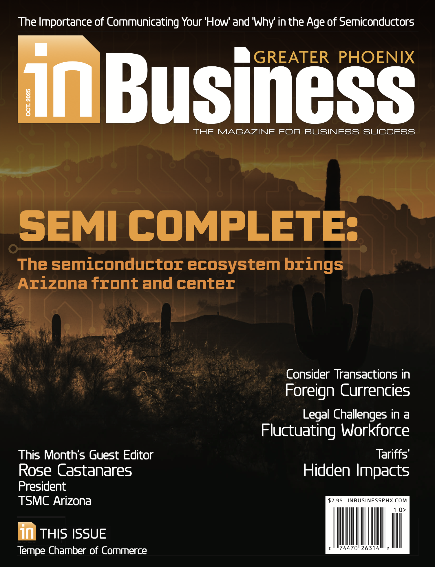

TSMC, the Arizona semiconductor fabrication facility, provided new information regarding their investment in TSMC Arizona.
“With the strong collaboration and support from our leading U.S. customers and the U.S. Federal, State and City governments, we recently announced our intention to invest an additional $100 billion in advanced semiconductor manufacturing in the United States, said chairman and CEO CC Wei regarding the Arizona update. ” This expansion includes plans for three additional wafer manufacturing fabs, two advanced packaging fabs, and a major R&D center.”
Combined with TSMC’s previously announced plan to build three advanced semiconductor manufacturing fabs in Arizona, this brings our total investment plan in the U.S. to $165 billion, to support the strong multi-year demand from our customers.
Their first fab in Arizona has already successfully entered high volume production in 4Q’24, utilizing N4 process technology, with a yield comparable to our fabs in Taiwan. The construction of their second fab, which will utilize 3-nanometer process technologies, is already complete, and they are working on speeding up the volume production schedule, based on the strong AI-related demand from customers.
The third fab will utilize N2 and A16 process technologies, and with the expectation of receiving all the necessary permits, is scheduled to begin construction later this year.
TSMC’s fourth fab will utilize N2 and A16 process technologies, and the fifth and sixth fabs will use even more advanced technologies. The construction and ramp schedules for these fabs will be based on customers’ demand.
TSMC also plan to build two new advanced packaging facilities and establish an R&D center in Arizona, to complete the AI supply chain. The expansion plans will enable TSMC to scale up to a GIGAFAB cluster, to support the needs of their leading-edge customers in smartphone, AI and HPC applications.
“With this additional $100 billion investment plan to expand our leading-edge capacity in Arizona,” said Wei, “I would also like to mention that TSMC is not engaged in any discussions with other companies regarding any joint venture, technology licensing, or technology transfer and sharing.”
After completion, around 30% of our 2-nanometer and more advanced capacity will be located in Arizona, creating an independent leading-edge semiconductor manufacturing cluster in the U.S. It will also create greater economies of scale, and help foster a more complete semiconductor supply chain ecosystem in the U.S.