When Nvidia and TSMC Arizona marked the first Blackwell wafer produced in Phoenix in October 2025, Nvidia CEO Jensen Huang called it “the very first time in recent American history that the single most important chip is being manufactured here.”





It was a milestone. It was also, in one important sense, unfinished.
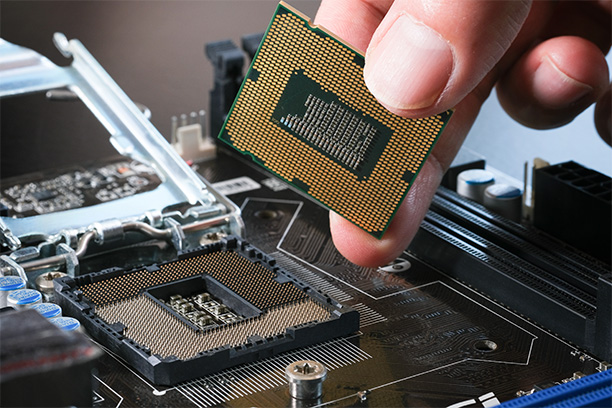
A wafer is not yet a working chip. Before a processor can go into a phone, a laptop or an AI server, it has to be cut, assembled, connected and tested; the industry calls this packaging. “Packaging is the final critical step in manufacturing silicon chips,” Apple noted when it announced its American Manufacturing Program in August 2025.
For decades, that final step has happened almost entirely in Asia. The United States held just 3% of global assembly, test and packaging capacity in 2022, according to a 2024 report from the Semiconductor Industry Association and Boston Consulting Group.
That gap is now closing — and Peoria is where it is closing fastest.
Amkor Technology, one of the world’s largest outsourced packaging and test companies, first announced a roughly $2-billion facility in Peoria in late 2023. The U.S. Commerce Department later awarded the project up to $407 million in CHIPS Act funding, calling advanced packaging “a significant chokepoint in the semiconductor industry’s ability to meet the rapidly increasing demand.”
Amkor broke ground in 2025 on what became a $7-billion campus on 104 acres in Peoria’s Innovation Core, with Apple as its first and largest customer. In May 2026, the company added 67 adjacent acres. And on Sept. 8, Amkor announced a second phase that lifts its total planned investment to about $12 billion, adds roughly 60,000 square meters of cleanroom space and raises expected employment to more than 3,500.
“This next phase reflects the confidence our customers have placed in Amkor, the critical role advanced packaging plays in enabling the future of semiconductor innovation, and the strategic importance of our Arizona campus,” says Kevin Engel, Amkor’s president and CEO.
Phase 1 construction is scheduled to run through mid-2027, with production beginning in early 2028. Phase 2 is set to finish by the end of 2029. Amkor expects the campus to be the first high-volume advanced packaging facility of its kind in the United States.
The customer list explains the scale. In June, TSMC and Amkor signed a 10-year agreement for TSMC to buy advanced packaging and test services from Amkor in Arizona, building on a 2024 agreement that covered InFO and CoWoS — packaging technologies used in smartphone processors and AI accelerators. In July, Nvidia struck a $1.5 billion multi-year deal with Amkor that includes a prepayment to support the company’s U.S. expansion.
Apple, meanwhile, says it is on track to buy “well over 100 million” advanced chips from TSMC Arizona’s fabs this year. Once Peoria is running, far more of those chips can be finished a short drive from where they were made.
TSMC is building its own capability, too. Its Arizona plan, which the company now puts at $265 billion, includes two advanced packaging facilities and a research and development center alongside its fabs. TSMC says initial construction on its first Arizona advanced packaging fab began in early 2026.
In 2024, Arizona State University and Deca Technologies opened what they describe as North America’s first fan-out wafer-level packaging research and development center. The two now co-lead SHIELD USA, a CHIPS-funded project of up to $100 million focused on next-generation substrates, the layer that connects a chip to the rest of a system.
“This is a critical step for U.S. semiconductor independence, and it is the area of expertise in which we are in direct competition with China,” ASU President Michael Crow says.
The stakes are highest in artificial intelligence. The most powerful AI processors are built by stacking or stitching multiple chips together, and the capacity to do that work has been one of the industry’s tightest bottlenecks.
Arizona spent the past five years proving it could produce leading-edge wafers. The next few will test whether it can finish the job.
If Peoria’s timeline holds, a chip could soon go from bare wafer to finished product without ever leaving the Valley.
Milestones
- Nov. 2023: Amkor announces a $2-billion packaging plant in Peoria
- Oct. 2024: Amkor and TSMC agree to package TSMC chips in Peoria
- Sept. 2025: Amkor starts Phase 1 construction
- Early 2026: TSMC begins work on its first Arizona packaging fab
- Sept. 2026: Amkor’s Phase 2 lifts its investment to about $12 billion
- Early 2028: Amkor’s first production expected
By the Numbers
- $407 million: federal CHIPS funding for Amkor, plus $7 million for workforce training
- 170 acres: size of Amkor’s Peoria campus
- 1 million square feet: planned cleanroom space after Phase 2
- 3% to 5%: U.S. share of global assembly, test and packaging capacity, 2022 vs. 2032 projection