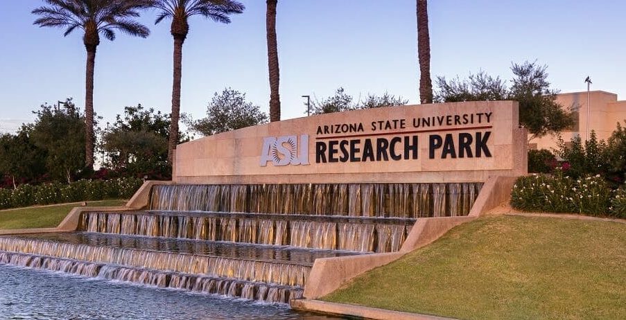
Inside the MacroTechnology Works facility at ASU’s Research Park in Tempe, a new kind of research center has opened: the Materials-to-Fab Center. This $270-million, world-class facility is designed to accelerate the transfer of innovations from lab ideation to fab-ready prototype, strengthening the bridge between academic research and real-world manufacturing. A ribbon-cutting ceremony marked the opening, bringing together Applied Materials executives, including Dr. Prabu Raja, president of the Semiconductor Products Group, with ASU President Michael Crow, Arizona Governor Katie Hobbs and other government and city leaders.


“The work of advancing discovery and, with it, the American semiconductor manufacturing industry, is of vital importance to the nation from both an economic competitiveness and a national security perspective,” said Arizona State University President Michael Crow. “The alliance between a global industry leader like Applied Materials and a leading research university like ASU and the work that will be done in the Materials-to-Fab Center will lead to breakthroughs and acceleration that enable chip manufacturers in the United States to lead the world in developing the technology that we need today and in the future.”
Applied Materials is the largest U.S. producer of semiconductor manufacturing equipment. Its tools are used to produce virtually every new chip in the world. The company’s major U.S. production facilities are located in Texas, Massachusetts and Montana, with a new site under development in Chandler, Arizona. The centerpiece of Applied’s R&D efforts is the EPIC Center in Silicon Valley, expected to become the world’s most advanced facility for collaborative semiconductor process technology and manufacturing equipment R&D when it opens in 2026.
“Universities are the foundation of America’s semiconductor innovation pipeline, and we look forward to bringing together ASU’s world-class engineering teams with Applied Materials technologists and ecosystem partners at the Materials-to-Fab Center,” said Dr. Prabu Raja. “These collaborations will focus on accelerating development of new chip technologies that are crucial to U.S. leadership in AI, high-performance computing and other megatrends shaping the future.”
ASU has become a national leader in advancing American microelectronics. With support from federal, state and private stakeholders, the university now plays a role across the entire semiconductor ecosystem, from early-stage innovation to advanced packaging and large-scale manufacturing. With the largest engineering school in the country, serving approximately 33,000 students, ASU is also a powerhouse in workforce and talent development.
“The Materials-to-Fab Center is a marriage made for Arizona and something that will benefit the entire region,” said Governor Katie Hobbs. “Applied Materials is an industry leader that already has a presence in the state, with many of its customers invested in doing work within the ecosystem that is growing here, and Arizona State University is a powerful force behind all the work being done, producing both the people who will lead this industry into the future and the ideas that will shape its progress. I am grateful to the Arizona Commerce Authority for helping this all come together and very excited to see this contribution to our economy coming to realization.”
“The launch of the Materials-to-Fab Center ushers in a new era for U.S. semiconductor innovation, providing a one-of-a-kind platform where innovators can test, refine and accelerate new processes and technologies,” said Sandra Watson, president and CEO of the Arizona Commerce Authority. “This pioneering collaboration between Applied Materials and ASU strengthens Arizona’s position as a national leader in semiconductor R&D, and we’re proud to support this transformative initiative.”
Arizona has emerged as one of the country’s most critical hubs for microelectronics. The state is home to leading semiconductor manufacturers, defense contractors, world-class research institutions and a fast-growing startup ecosystem. The Materials-to-Fab Center will serve as a key regional asset — benefiting companies of all sizes and connecting public and private investments in research, innovation and advanced manufacturing.
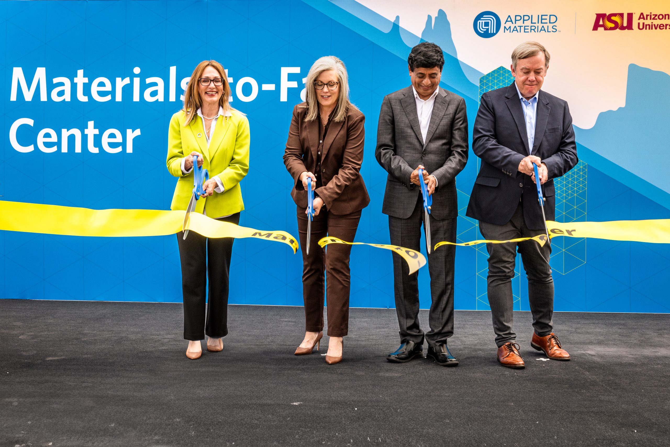 Caption: (L-R) Sandra Watson President and CEO, Arizona Commerce Authority; Governor Katie Hobbs; Prabu Raja, Ph.D., President, Semiconductor Products Group for Applied Materials; Michael Crow, President, Arizona State University. Photo by Charlie Leight, courtesy of ASU News
Critical Timeline
2023 – Partnership & Facility Announcement
ASU and Applied Materials publicly disclose their joint plan for the Materials-to-Fab Center at MacroTechnology Works, projecting a two-year development timeline.
Mid‑2023 to 2024 – Design and Planning Phase
Design work and project planning proceed, supported by funding commitments and stakeholder alignment.
2025 – Buildout and Equipment Installation
By 2025, the building infrastructure and necessary semiconductor processing equipment begin to be installed and readied for operation.
October 9, 2025 – Grand Opening
The $270 million Materials-to-Fab Center opens with a ceremonial ribbon cutting. ASU, Applied Materials and Arizona leadership highlight its role in accelerating translation from research to prototype.